PCB substrate CCL

This time let’s to know the PCB substrate CCL. CCL also known as the PCB substrate. The reinforcement material impregnated with resin, one or both sides covered with copper, made by hot pressing into a  plate material, as copper clad laminates.

It is to do the basic PCB material, often called the substrate CCL. When it is used for multilayer circuit board production, also called core board (CORE).

FR-4 —- Flame Resistant Laminates,our material is now commonly used FR-4, also the most popular used for substrate.

PCB outline processing technology

People Who engaged in printed circuit board processing, will be understanding: PCB outline processing is one of the difficulties of the whole PCB processing , most PCBS ARE a rectangle outline, but also a considerable number of PCB with special outline.

Please see the below four PCB outline processing methods:

1. Milling outline: PCB outline processing by CNC milling machine, we should be provides the data of outline and the corresponding hole, and it will be input by programmer. As not so much distance between PCB puzzle, usually about 3mm, so mills generally 3mm in diameter, or 2.4mm. First milling drill hole on the plate, then fixed the PCB and plate, last milling outline.

2. Punching outline: Need to setup mold, then punching outline, correspond the PCB positioning pin and the positioning hole, generally choosing 3.0mm hole as positioning hole.

3. Open “V” groove: Using “V” groove cutting machine along the PCB design “V” slot cut into the PCB parts connected to each other;

4. Drill outline: Using drill machine to drill holes through outline. Normally open “V” groove and drill only for processing assistance.

CMD Circuit specilizing in making high quality printed circuit boards and flexible circuits. Please contact us to know more.

Flexible Circuits Price

Almost all the electronics factory purchasement staff have been confused about the changing price of flexible circuits, even if some have many years of experience in the purchasement of flexible circuits  staff has not totally understand the causes. In fact, the price of flexible circuit board by the following multi- factors:

1, flexible circuit boards of the multifarious price caused by different material;
2, flexible circuit boards used in the different production process caused by the multifarious price;
3, the difficulty of flexible circuit board itself caused the multifarious price;
4, customer different requirements will result in different prices;
5, different flexible circuit board manufacturers will course multifarious price;
6, different method of payment of price will course multifarious price;
7, different regional also will course multifarious price.

You can see the above main seven factors consist of flexible circuit boards price. If you have an inquiry about the flexible circuit boards, please don’t hesitate to contact us, we will offer you the very competitive price.

Exposed copper of HASL analysis and treatment

As you know, the HASL is the most popular PCB surface treatment,exposed copper maybe be coursed by this method.

HASL is that input the PCB in molten solder (63SN/37PB), then use hot air to blows off the excess solder in the surface and metal-based inner hole of printed circuit board to get a smooth, uniform and also bright solder plated layer. After HASL surface treatment of printed circuit board the plated layer should be bright and uniform integrity, good weldability, without nodules and half-wetting,plated layer is complete no exposed copper.

After HASL, pad surface and the metal-based inner hole are exposed copper is an important test of finished product defects, also is the one of main reasons of HASL rework. please see the below several reasons for exposed copper:

1. Pad surface dirty, contaminated with residual solder pad.
2. Pre-treatment is not enough, coarsening bad.
3. Flux activity is not enough.

We should control the technology of exposed copper of HASL surface treatment, reduce the Rework and poor circuir boards, ensure the quality of products.

PCB to prevent warping

How to prevent the PCB warping? This is the most improtant in the PCB manufacturing preocess.

1. Why is flat circuit board requirement

In the automation plug line, if PCB isn’t flat will cause mispositioning, components can not plug in to the board of the hole and surface mount pad, and even crashing automatically installed machine. After components installed on board, component pins are difficult to cut neatly. Board can not be fitted to the chassis or the machine’s outlet, so, board assembly factory is also very troubled.

2. Warpage standards and test methods

According to the U.S. IPC-6012 (1996 Edition) <<Rigid Printed Boards and performance specifications>> for the maximum allowable surface mount PCB warpage and distortion of 0.75%, other 1.5% of various board permitted. Compare to IPC-RB-276 (1992 Edition) to improve on the requirements of surface mount PCB. Currently, the electronic assembly factory agree with, regardless of double or multi, 1.6mm thickness, is usually 0.70 to 0.75%, and for SMT, BGA’s board, demand is 0.5%.
 
3. Warping board processing:

As in our factory, PCB in the final test will be 100% flatness inspection. Failure of the board who will be singled out, into the oven at 150 degrees and bake under the weight of 3 to 6 hours, and under the weight of natural cooling. And relieving the board out, check in for smoothness, this would save parts of the board, some boards need to bake for two to three times the pressure to leveling.

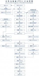
Flexible Circuits Production Process

Last time we talk about the PCB production process, now please see the below form of flexible circuits production process for you study.

CMD Circuits has a very strict quality control system to ensure to make high quality flexible circuits. Please feel free to contact us for any queries.

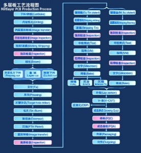
Multilayer PCB Production Process

If you want to know more details of the PCB production process, now please see the below form of our multilayer pcb production process for you study.


CMD Circuits has a very strict quality control system to ensure to make high quality products.

Why to use high Tg PCB Material?

First of all, talk about the high Tg refers to the high heat resistance. With the rapid development of electronic industry, especially on behalf of computer electronic products toward the high function, high-rise development, require higher PCB material heat resistance as an important guarantee. With SMT, CMT represented by the emergence of high-density mounting technology and development, and the PCB in the small hole size, fine lines, thinner, the more inseparable from the support substrate with high heat resistance.

PCB materials under high temperature, not only produce softening, deformation, melting and other phenomena, but also in the mechanical, electrical characteristics of the sharp decline (I think we do not want to see their products occurred).

So the general high-Tg FR-4 and the difference between the FR-4: In the thermal state, especially in the heat after absorption, its materials, mechanical strength, dimensional stability, adhesion, water absorption, thermal decomposition , thermal expansion differences in various situations, high Tg products significantly better than the common PCB materials. This is why to use the high Tg PCB material.

PCB surface treatments

Bare copper itself is very good solderability, but is easily exposed to air oxidation, and susceptible to contamination. This is also the PCB surface treatment must be the reason.

1. HASL
Hot-air solder leveling. The most common PCB surface treatment menthod. Lead and lead-free should be considered.

2. OSP
Organic solderability protective coating (OSP, Organic solderability preservative) is an organic coating to prevent oxidation of copper in the welding before, that is to protect PCB(printed circuit board) pad solderability from destruction.

3. ENIG
Nickel Immersion Gold. The copper surface is plated of Ni/Au. The deposition thickness of the inner Ni layer is generally 3~6um, the deposition thickness of the outer Au thin, usually 0.05 ~ 0.1um. Ni as the barrier layer between Cu and soldering tin. Welding, outside Au in the solder which melts rapidly with soldering tin and then turn into Ni/Sn intermetallic compounds with inner Ni. The gold-plated to prevent Ni oxidation during storage or passive, it should be enough gold plating density, the thickness can not be too thin.

4. Immersion Silver
Immersion silver process through the thin (about 0.1~0.4um) and dense to provide a layer of silver deposited organic protective film, the surface of the silver with the greatly extended life. Immersion Silver surface is very flat and very good with weldability.

5. Immersion Tin
Only used for two reasons for immersion tin process: first, the surface is very flat, coplanarity good; the other is lead-free. But in the immersion tine process easy to be with Cu/Sn intermetallic compound, Cu / Sn intermetallic is with poor solderability.

These are five main PCB surface treatments, since each have their own unique surface treatment technology, application is not quite the same.
the whole thickness of FPCs

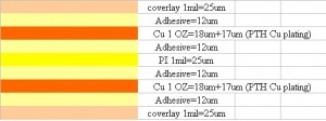
Now I want to introduce the wholes thickness of FPCs. As is known to all, there are four kinds of FPCs(flexible circuits): single-sided FPC, double-sided FPC, dual access FPC and multiayer FPC. Let’s see the thickness of single-sided and double-sided FPC as examples:

(!) single-sided FPC

The constructure of single layer FPC is as follows:

25um+20um+35um+20um+25um=125um≈0.12mm

Note: the thickness of adhesive changes according to the thickness of Cu. For 1/2, 1/3 OZ Cu, we usually use 12um adhesive. But for 1OZ Cu, we have to use 20um adhesive.

That’s according to the common material. If we want the board to be thinner, we also can use the adhesiveless material to make the board about 0.60mm thick.

(2) double-sided FPC

Double sided FPC means there are two layer of traces in the FPC.

The constructure of double sided FPC is as follows:

25+12+35+12+25+12+35+12+25=193um≈0.20mm

Now you have an idea about the whole thickness of the FPCs, if you need more information, please contact us anytime.

Pages: Prev 1 2 3 4 5 6 7 Next