Monthly Archives: September 2010

The stiffener of flexible circuits

The characteries of flexible circuits are thin, light weight, but easy to happen folding, scars in the process of using, and mechanical strength is small, easy to crack. Stiffener is intended to strengthen the mechanical strength of flex circuits, easy to install surface components.

Stiffener has a variety of types, according to requirements of using, mainly have PET, PI, adhesive, metal or resin reinforcement plate, etc.

There have two ways to press stiffener of flexible circuits:

1. Hot pressing of stiffener: Using high temperature to melt adhesive film of stiffener, then use of appropriate pressure or vacuum to closely fit the stiffener film on the products;
2. Sensitive pressure of stiffener: no heating, products pressure through the cold pressing machine.

PCB silk screen plate making process

Please see the below  PCB silk screen plate making process:

1.Stretching

Stretching steps: network clean – the level of calibration – the bottom of plastic coated – Pop – Tension Measurement – coated adhesive – the net, Edge – Storage.

2.Drying net

Wash Network – Drying – use of premium film method – using light-sensitive adhesive (net pulp) – the choice of mesh lines – Film’s choice – exposing – Pressurized water wash and dry – use blue oilto cover – inspection, repair network, write the date of completion and the corresponding number and record keeping, storage.

3.Storage

Storage has generally adopted a vertical storage, network framework can be made or purchased, should be stored in the same environment with the screen environment to prevent deformation, while the screen before the need to test the tension on the screen, and test by the photographic film .

Silk-screen production steps

This time follow me to know the silk-screen production steps, how to mak e the silk-screen of printed circuits boards.

First, wash silk-screen

* Items required for washing silk-screen:
1, stripping water;
2, diluent;
3, detergent.

Second, coating

* Required coating materials: photoresist, scraper bucket, frame net sets.

Third, how to prepare light-sensitive adhesive.

Fourth, exposure.

Last, develop, wash csreen, drying and repair.

These are the silk-screen production steps, CMD Circuits has many years of experience of making printed circuit boards. Please contact us to know more.

PCB testing

This time let’s to talk about the PCB testing. When the printed circuit boards are finisehd, we should test PCB for short or open circuit condition, we can use optical test or E-test way to test.

Optical test methods identify defects in each layer by scanning, the electronic testing is usual using Flying flying-probe to check all connections. E-test for short circuit or open circuit much more accurate, but the optical test can more easily detect incorrectgap problems between conductors.

CMD Circuits have the very strict quality control and testing machines, please don’t worry about the quality of our circuit boards.

PCB copy board methods and steps

As you know, sometimes we will face to copy pcb as our customers just have the pcb circuit board samples in hand, no gerberfile. Please see below details of the PCB copy board methods and steps.

The first step, get a piece of PCB, keep records on paper of all molds, parameters, and location of the components, especially direction of diode, three machine and IC gap. Best to use digital camera to take photoes of the locations.

The second step, remove all the components, and remove the tin in PAD hole. Then use alcohol to clean printed circuit board, and then turn into the scanner,start POHTOSHOP, with a color screen to scan the silk screen side, save the file and print out.

The third step, use the water tissue paper to top layer and bottom layer minor sanding, grinding to a shiny copper film, into the scanner, start PHOTOSHOP, two color ways were swept. Note, PCB placed in the scanner must be horizontal level within the tree, otherwise the scanned image will not be able to use, and save the file.

The fourth step is to adjust the contrast of the canvas, with strong conparison between the copper film and no copper film part, then turn second picture to black and white color, check the lines are clear, if not clear, repeat this step. If clear, save the picture into black and white BMP format: TOP.BMP and BOT.BMP, if found in graphics problems can be repaired and modified with PHOTOSHOP.

The fifth step, turn these two files converted to PROTEL format, in PROTEL with two layers, if the PAD and VIA of two layers are on the same plase is means that the first few steps do well, if biased, then repeat the third step.

Sixth, Turn the TOP layer of BMP into TOP.PCB, attention should be transformed to the silk layer, that layer is yellow, and scan the top layer, and place the components according to the second step of the drawings.

Seventh step, turn the BOT layer of BMP into BOT.PCB, attention should be transformed into SILK layer, that layer is yellow, and scan the top layer. Deleted silk layer when finished.

Eighth step, Let TOP.PCB and BOT.PCB together in PROTEL, merged into a graph, it’s OK.

The ninth step, use a laser printer to print TOP LAYER, BOTTOM LAYER to a transparent film on the (1:1 ratio), put the film onto the PCB, compare to them, if right, you’re done .

Other: If it’s a multi-layer pcb, we should repeat the third to the ninth step, of course, named of the graphic is different, based on the number of layers. It’s much simpler to copy multi-layer double-sided pcb than multi-layer pcb.

Ok, these are the ninth steps of the double-sided pcb copy menthods, for more information, please contact us.
The shortcomings of FPC characteristics

As your know, Flexible circuits(FPC) provide major benefits over rigid circuit boards, but they also have the shortcomings. Please see below shortcomings of FPC Characteristics:

1. Small mechanical strength,easy to crack;
2. Difficulties in process design;
3. The possibility of re-processing is low;
4. The difficulties for checking;
5. Can’t Carrying heavy parts for single one;
6. Easy to break, beat, wound;
7. Higher cost of the product.

Althrough FPC have these shortcomings, but now more and more widespread use of Flex circuits, more and more advanced technology. We can develop the strong points and avoid the weak points and provide quality goods at competitive cost.

Flexible circuit substrate thickness

This time let’s to see the several kinds of based flexible circuit substrate thickness, & then you can see which is the best suitable for you.

1. Coverlayer of flexible circuits:

1). 12.5um: PI:12.5um; adhesive:15um; total thickness: 27.5um
            PI:12.5um; adhesive:25um; total thickness: 37.5um
2). 25um:   PI: 25um;  adhesive:25um; total thickness: 50um

2. Substrate thickness of flex circuits

1).Single RA copper:

18/12.5UM: copper thickness:18um; PI:12.5um;adhesive:13um; total thickness 43.5um
35/25UM:  copper thickness:35um; PI:25um; adhesive: 20um; total thickness 80um

2).Double-sided RA copper:

18/12.5UM: copper thickness:18um; PI:12.5um; adhesive: 13um; total thickness: 74.5um
35/25UM: copper thickness:35um; PI:25um; adhesive: 20um; total thickness: 135um

I think we have all of your required thickness, we haven’t any problem to product it according to your requirements. OK, if you need further information of flexible circuits(flex pcb), please contact us feel free.

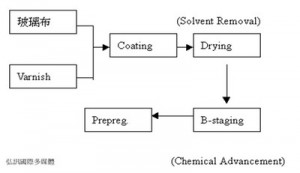
Prereg Making Process

Prereg also named “bonding sheet” (adhesive film), it’s the main part of the pcb substrate CCL, and made by glass fiber or other impregnated resin fibers.

Please see the blow form of prereg making process: